The flash memory is connected to the i960RP memory controller. For details applicable to the flash, see the i960RP Microprocessor User's manual, chapter 14, sections 14.1-14.4.
![]()
Table 1: Physical Memory Configuration for FLASH Memory
The FLASH memory installed on the ISE board is a SST 28SF040. This is
an 8-bit wide device, connected to the i960RP local bus and CE0#. The
settings of PMCON in Table ![]() configure the region
correctly. See the i960RP Microprocessor User's Manual,
Section 12.2-Programming the Physical Memory Attributes.
configure the region
correctly. See the i960RP Microprocessor User's Manual,
Section 12.2-Programming the Physical Memory Attributes.
The flash memory contains the initial memory image for bootstrap, and the i960RP uses the CE0# chip select to access the device. Only the low order 19 address bits are connected to the memory chip, so the flash repeats within the address space. The i960RP initially accesses the flash on the ISE board at the top of a 16MByte region.
After reset, the flash is mapped by default register settings into the 16MByte region at 0xfe000000. Typically, flash images are linked into the range 0xfef80000 - 0xfeffffff (512 KBytes). Since addr19-31 are ignored by the flash, the address of 0xfef80000 correctly accesses the beginning of the memory, even with the default configuration register settings. The canonical setting for the base address register then should be as in
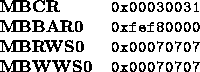
Table 2: Memory Control Configuration for FLASH Memory
Table ![]() , although the default value of MBAR0 (
0xfe000000) works perfectly well, at the expense of 15MBytes of
address space.
, although the default value of MBAR0 (
0xfe000000) works perfectly well, at the expense of 15MBytes of
address space.
See the i960RP Microprocessor User's Manual, Section 14.4-Memory Bank Programming Registers.
The flash memory is a slow device, so the maximum read and write wait states must be inserted. Also, the MBCR, which sets the width of the region, must be set after MBBAR0 is set, or the flash will become inaccessible.
If the program is expected to write to the flash memory, the last byte of the MBCR should be changed from 0x31 to 0x33 to make the region writeable. This should normally be left read-only to prevent accidents.